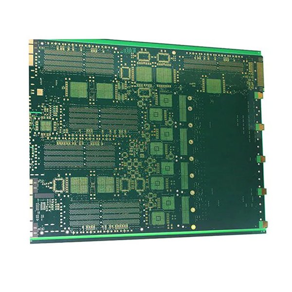
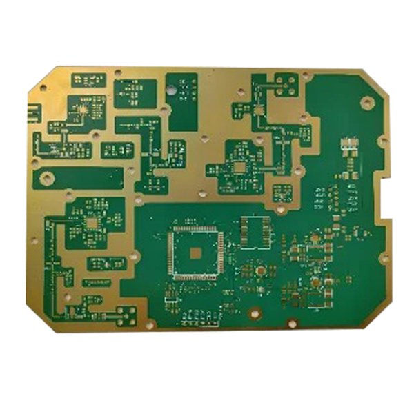
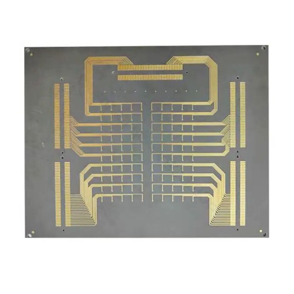
8L Microwave PCB Isola Astra MT77
Overview
Microwave printed circuit boards (PCBs) are specialized substrates optimized for use at microwave frequencies, typically defined as signals exceeding 1 GHz. This technology plays a crucial role in facilitating high-frequency wireless communications, radar systems, electronic warfare, and testing equipment, operating effectively at millimeter wave frequencies up to 100 GHz.
Benefits of Microwave Printed Circuit Boards
Utilization of Low-CTE Materials: These materials help stabilize PCBs in high-temperature conditions.
Flawless Layer Alignment: Ensures a smooth and precise alignment of various layers.
Alignment of Multiple Layers: Low CTE materials facilitate the alignment of numerous layers within intricate structures.
Reduced Assembly Costs: Helps lower overall production expenses.
Enhanced Performance: Delivers optimal functionality.
Better High-Frequency Signal Transmission: Improves the efficiency of signal transmission at high frequencies.
Supports More Complex Designs: Allows for the creation of intricate and sophisticated designs.
Microwave PCB Fabrication and Assembly
The creation of microwave printed circuit boards involves sophisticated manufacturing techniques and assembly methods:
Material Evaluation: Properties such as dielectric constant and loss tangent are thoroughly assessed on production panels to ensure quality.
Surface Treatment: Oxide treatments and chemical preparations are employed to improve copper adhesion.
Etching Techniques: Conductors are formed using printed, plated, or etched methods to achieve intricate designs with smooth contours.
Layer Alignment: Precise alignment during layer stacking and lamination minimizes parasitic effects.
Hole Quality Assurance: Drilling techniques ensure high-quality hole walls for dependable plated via connections.
Solder Mask Application: A photoimageable mask offers excellent spatial accuracy for enhanced component placement.
Pad and Gap Specifications: Conductor layouts are precisely matched to chip terminations within micrometer tolerances.
Plating Supervision: Stringent control over plating thickness and hole filling maintains consistent electrical performance.
Automated Evaluation: Comprehensive electrical testing verifies impedance, signal propagation, and resonant frequencies.
Controlled Assembly Processes: Surface Mount Technology (SMT), wire bonding, and conformal coating are executed according to established protocols.


