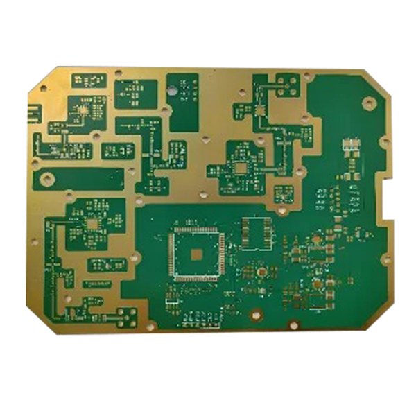
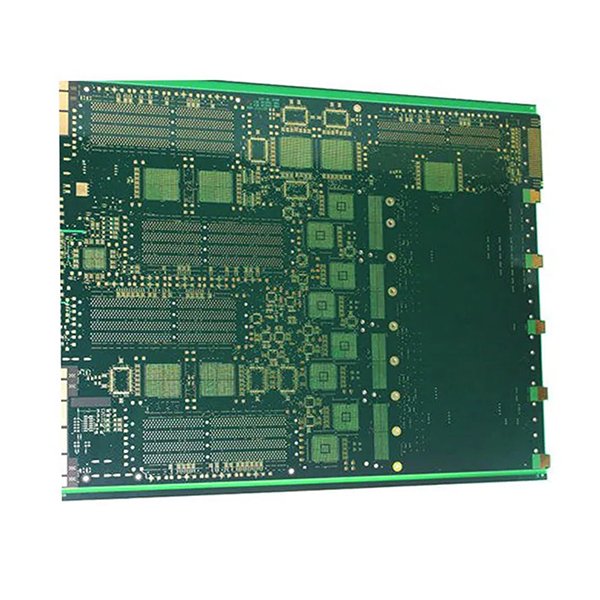
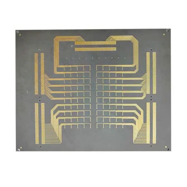
4L Microwave PCB Arlon CLTE-XT
What are Materials Used in Microwave PCBs?
The choice of substrate material is critical in microwave PCB design. Common materials include:
1. Rogers RO4000 series: Low-loss, temperature-stable materials
2. Taconic RF-35: High-frequency laminates with low dielectric constant
3. Isola Astra MT77: High-performance materials for millimeter-wave applications
4. Arlon CLTE-XT: Low-loss materials with excellent thermal stability
Here's a comparison of some popular microwave PCB substrate materials:
Material | Dielectric Constant | Dissipation Factor | Frequency Range |
Rogers RO4350B | 3.48 | 0.0037 | Up to 40 GHz |
Taconic RF-35 | 3.50 | 0.0018 | Up to 77 GHz |
Isola Astra MT77 | 3.00 | 0.0017 | Up to 100 GHz |
Arlon CLTE-XT | 2.94 | 0.0012 | Up to 110 GHz |
Key Points in Microwave PCB Manufacturing
Etching Techniques
Accurate etching is vital for microwave PCBs to ensure precise trace widths and spacing. Advanced etching methods include:
1. Laser Etching: Provides high precision for intricate features.
2. Chemical Etching: Effective for larger features and lower frequency applications.
3. Plasma Etching: Delivers clean, precise edges ideal for high-frequency uses.
Lamination and Bonding
The lamination process is essential for preserving the integrity of the substrate material and ensuring proper adhesion between layers. Important factors to consider include:
1. Temperature Control: Helps prevent warping and maintains material properties.
2. Pressure Uniformity: Ensures consistent bonding throughout the board.
3. Vacuum Lamination: Eliminates air pockets and enhances layer adhesion.
Drilling and Via Formation
Vias are crucial in microwave PCBs for grounding and connecting layers. Advanced drilling methods include:
1. Laser Drilling: Ideal for small, high-aspect-ratio vias.
2. Mechanical Drilling: Suitable for larger vias and through-holes.
3. Back-Drilling: Removes unused sections of plated through-holes.
Plating Processes
Plating is key for forming conductive vias and enhancing surface conductivity. Common plating methods include:
1. Electroless Copper Plating: Provides the initial layer for via walls.
2. Electrolytic Copper Plating: Increases copper thickness.
3. Nickel and Gold Plating: Used for surface finishes and improved conductivity.


