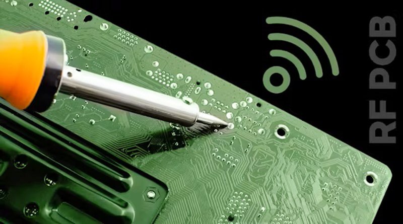
RF PCB Prototypes: Understanding Data Requirements, Review Factors, and Lead Times
Introduction to RF PCB Prototypes
RF PCB (Radio Frequency Printed Circuit Board) prototypes serve as crucial tools for validating concepts and ensuring that the designs will perform as expected in real-world applications. As RF technology continues to evolve, prototyping has become a vital step in developing reliable high-frequency devices, including telecommunications, medical equipment, and IoT devices. This article explores the necessary data requirements for RF PCB prototypes, factors to consider when reviewing prototyping data, and typical lead times involved in the prototyping process.
Data Requirements for RF PCB Prototypes
Creating an effective RF PCB prototype requires comprehensive data to ensure functionality and performance. The following data sets are essential for achieving a successful prototype:
Schematic Files
Detailed schematics outline the electrical connections and functionality of the PCB. This should include all components, such as resistors, capacitors, and RF inductors, along with their connections.
Layout Files
The layout, often created in a PCB design software tool, must include the physical placement of components, routing of signal traces, vias, and ground planes. Common file formats include Gerber, ODB++, or IPC-2581.
Stack-Up Information
Clear documentation of the layer stack-up, including the number of layers, thicknesses, and material specifications (e.g., dielectric constant, loss tangent), is crucial for controlled impedance and overall performance.
Impedance Requirements
Specific details regarding the desired characteristic impedance (commonly 50 ohms or 75 ohms) for traces and connections, along with calculations used to achieve these results.
Bill of Materials (BOM)
A comprehensive BOM lists all components, their specifications, part numbers, and suppliers. This document is essential for sourcing and inventory management during prototype assembly.
Assembly Instructions
Step-by-step guidelines on how to assemble the components onto the PCB, including soldering techniques and any specialized assembly processes (e.g., surface mount or through-hole).
Test Plans
Documentation of expected testing procedures and test points on the PCB for performance validation, including tests for gain, loss, and signal integrity.
Factors to Consider When Reviewing RF PCB Prototypes Data
When reviewing RF PCB prototypes data, it is critical to assess multiple aspects to ensure quality and performance:
Design Rule Compliance
Verify that the prototype adheres to established design rules and standards, including minimum trace width, spacing, and pad sizes. This step helps prevent manufacturing defects and performance issues.
Simulation Results
Review the outcomes of any electromagnetic simulations performed on the PCB layout. Ensure that critical parameters such as return loss, insertion loss, and worse-case scenarios have been analyzed comprehensively.
Impedance Matching
Ensure that the impedance requirements outlined in the design have been accurately implemented. Proper impedance matching is crucial for reducing signal reflections and maintaining signal integrity.
Component Quality and Tolerance
Assess the quality and specifications of all components listed in the BOM. Ensure that the selected components can withstand the environmental conditions and frequency ranges for optimal performance.
Thermal Management
Evaluate the thermal analysis data regarding how heat will be dissipated in the design. Consider whether proper measures, such as heat sinks or thermal vias, have been incorporated.
Testing Procedures
Review the proposed testing plans to ensure that they adequately cover all critical performance metrics. This includes assessing the methodology for validating RF performance against expected specifications.
Documentation Clarity
Ensure that all documentation presented is clear, organized, and comprehensive. Proper documentation aids in assembly, testing, and future revisions of the design.

General Lead Time for RF PCB Prototypes
The lead time for producing RF PCB prototypes can vary widely based on several factors, including complexity, manufacturing capability, and supplier resources. However, a general breakdown can be outlined as follows:
Design Phase:
The design and validation phase typically takes 1-3 weeks, depending on the complexity of the PCB, revisions required, and the availability of simulation resources.
Manufacturing Time:
After finalizing the design, the manufacturing lead time for RF PCBs generally ranges from 2-4 weeks. This can vary based on factors such as layer count, material specifications, and the capacity of the manufacturing facility.
Assembly Process:
Once the PCB is manufactured, assembling the components usually takes an additional 1-2 weeks. The complexity and the number of components can significantly affect this timeframe.
Testing and Validation:
Post-assembly testing and validation may take another week, depending on the extent of the testing procedures and if any issues arise during initial evaluations.
Conclusion
RF PCB prototyping is a critical step in the development of high-frequency devices. By understanding the specific data requirements for prototypes, carefully reviewing the data and designs, and being aware of lead times, designers and engineers can enhance their prototyping processes. This ultimately leads to more reliable RF devices, ensuring performance and functionality in various applications. As the demand for RF technology continues to grow, adopting a meticulous approach to PCB prototyping will remain essential for success in this competitive landscape.
 The Need for Rogers PCB Materi
 Eco-Friendly PCBs: How the Ind
 How PCB Manufacturers are Inno
 High-Frequency PCBs: The Key t
