RF PCB Impedance Control: Understanding, Standards, and Manufacturing Considerations
Introduction to RF PCB Impedance Control
Impedance control is a critical aspect of designing RF (radio frequency) PCBs (Printed Circuit Boards). It refers to the practice of ensuring that the impedance of transmission lines—such as traces, microstrips, and striplines—remains consistent throughout the PCB. Proper impedance control is essential for minimizing signal reflections, maximizing power transfer, and ensuring the integrity of high-frequency signals that RF PCBs typically handle. This article explores the meaning of RF PCB impedance control, the standard requirements for it, and considerations to maintain impedance control during manufacturing.
What Does RF PCB Impedance Control Mean?
RF PCB impedance control involves designing the board layout and selecting materials to achieve and maintain specific impedance values, commonly 50 ohms or 75 ohms. These values are critical for various RF applications, including telecommunications, radar systems, and wireless communications.
The concept stems from the need to manage how signals travel along transmission lines:
Reflection: When the impedance of the transmission line does not match the load (e.g., an antenna or another circuit), some signal energy is reflected back toward the source, leading to loss of signal integrity.
Signal Integrity: Keeping the impedance consistent ensures that the signal can propagate without unwanted distortions or losses, which is particularly vital in high-speed applications.
Standard Requirements for RF PCB Impedance Control
The industry has established several standard requirements for RF PCB impedance control, designed to ensure optimal performance:
Characteristic Impedance: Most RF applications adhere to standard impedance values, typically 50 ohms in high-frequency communication systems or 75 ohms for video and broadcast applications. Designers must maintain this specification throughout the PCB to prevent signal degradation.
Impedance Tolerance: Most RF designs aim for a tolerance of ±10% or better. This means that the actual impedance of the transmission line should fall within 45 to 55 ohms for a 50-ohm line.
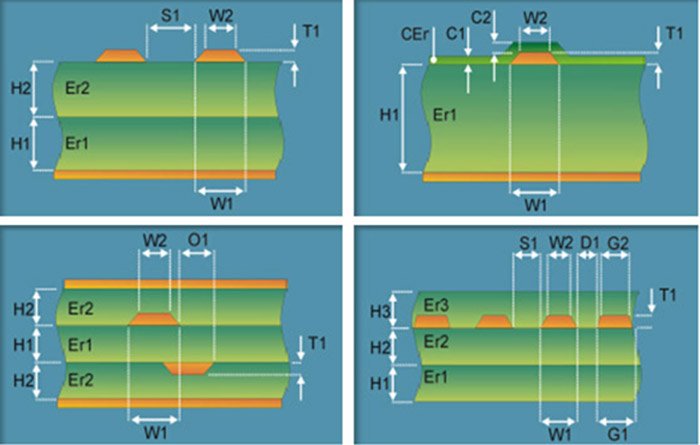
Controlled Impedance Design: PCBs should be designed using tools capable of calculating and adjusting trace widths, dielectric thickness, and spacing to achieve the desired impedance.
Testing Procedures: Standard testing methods such as TDR (Time Domain Reflectometry) and VNA (Vector Network Analyzers) should be implemented to verify impedance after manufacturing, ensuring compliance with the designed specifications.

Considerations for Maintaining RF PCB Impedance Control During Manufacturing
To achieve and maintain proper RF PCB impedance control throughout the manufacturing process, several factors must be taken into account:
1. Layer Stack-Up Design
Layer Configuration: Design the stack-up with careful consideration of dielectric materials, thickness, and placement of signal layers. A common configuration involves RF signal traces on outer layers, with power and ground planes providing shielding and reference.
Dielectric Material: Choose low-loss dielectric materials with stable dielectric constants (Dk) to ensure consistent impedance over frequency variations.
2. Trace Width and Spacing
Trace Geometry: Use PCB design tools to accurately simulate trace width, spacing, and the total thickness of the dielectric material. This ensures the traces have the correct width to meet the target impedance.
Vias: Design vias carefully to minimize inductance, ensuring they do not significantly affect the impedance along transmission lines.
3. Fabrication Process Control
Material Consistency: Work with reliable suppliers and manufacturers to ensure that the dielectric materials and copper foil used in the PCB fabrication process have consistent properties. Variability can lead to unexpected impedance changes.
Manufacturing Tolerances: Maintain strict tolerances in the manufacturing process, as variations in copper thickness or dielectric layer thickness can significantly impact impedance.
4. Testing and Verification
Pre-Manufacturing Simulation: Use electromagnetic simulation tools to model the PCB's behavior before manufacturing. This can help predict how impedance will be affected by design choices.
Post-Fabrication Testing: Employ techniques such as TDR and VNA testing on completed boards to verify that the impedance of transmission lines meets specifications before deploying the PCB into an operational environment.
5. Environmental Considerations
Thermal Effects: Understand how temperature fluctuations might influence dielectric properties. Select materials that have stable thermal characteristics to maintain impedance consistency under varying conditions.
Moisture and Humidity: Consider the effects of environmental conditions on the PCB materials. Moisture can alter the dielectric constant, potentially affecting impedance.
Conclusion
Impedance control in RF PCBs is a fundamental aspect of ensuring signal integrity and performance in high-frequency applications. By thoroughly understanding what impedance control means, adhering to established standards, and actively considering manufacturing practices, designers can significantly improve the reliability and efficiency of RF circuits. With the continued growth of wireless communication technologies and RF applications, proper impedance control will remain a pivotal focus in PCB design and manufacturing processes.
 The Need for Rogers PCB Materi
 Eco-Friendly PCBs: How the Ind
 How PCB Manufacturers are Inno
 High-Frequency PCBs: The Key t
