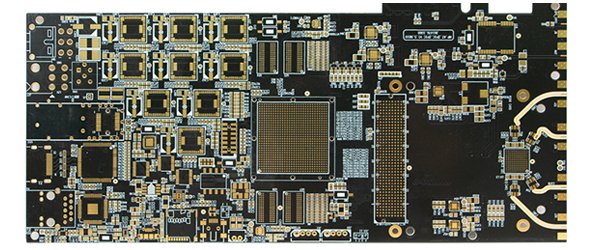
RF PCB Design: Radio Frequency Printed Circuit Boards

Frequency Considerations:
One of the primary factors to consider when developing an RF PCB design is the operating frequency range. The choice of frequency range influences the selection of components, material characteristics, and routing techniques. RF circuits typically operate at high frequencies, often ranging from a few Megahertz to several Gigahertz.
To ensure optimal performance, it is crucial to carefully select the appropriate PCB material with low dielectric loss and consistent impedance characteristics across the frequency spectrum. High-frequency laminates such as Rogers or Taconic materials are commonly used for RF PCB designs due to their excellent electrical properties.
Additionally, proper trace width and spacing become critical at higher frequencies to maintain controlled impedance. Transmission lines, such as microstrips or strip lines, should be designed with precise dimensions to match the desired characteristic impedance. Utilizing controlled impedance calculators or specialized design tools can aid in determining the optimal trace dimensions.
Key Considerations in RF PCB Design:
1. Impedance Matching:
Impedance matching is crucial in RF design to maximize power transfer and minimize signal reflection. Designers must carefully control trace widths, spacing, and dielectric thickness to maintain consistent impedance throughout the signal path.
2. Transmission Line Design:
Microstrip and stripline configurations are common in RF PCB design. Microstrip lines are typically used for simpler designs, while striplines offer better EMI shielding but are more complex to implement.
3. Grounding Techniques:
Proper grounding is essential in RF designs to minimize noise and ensure signal integrity. Techniques such as ground planes, stitching vias, and careful component placement play a vital role in effective grounding.
4. Component Selection and Placement:
Choosing the right components and placing them optimally is critical. High-quality, low-tolerance components should be used, and sensitive components should be placed away from potential sources of interference.
5. EMI/EMC Considerations:Electromagnetic Interference (EMI) and Electromagnetic Compatibility (EMC) are significant concerns in RF design. Proper shielding, filtering, and layout techniques are essential to minimize interference and ensure compliance with regulatory standards.
RF PCB Materials:
FR4 materials are acceptable for RF transmission lines and interconnects operating up to WiFi frequencies (~6 GHz). Beyond these frequencies, RF engineers recommend using alternative materials to support RF signal propagation and printed RF circuit designs. Standard FR4 laminates use resin-filled fiberglass weaves to hold components, but these fiber weave effects in certain materials could create signal and power integrity problems if fabrication procedures are not specified properly.
RF PCBs are manufactured with certain materials that fulfill high-frequency operation requirements. These materials should have low signal losses, be stable over high-frequency operation, and should be able to absorb high amounts of heat. The dielectric constant (DK), loss tangent (tan δ), and coefficient of thermal expansion (CTE) values also require consistency over wide frequency ranges. Typical values of dielectric constant range from 3 to 3.5 for these boards. Loss tangent values are in the range of 0.0022 to 0.0095 for the frequency range of 10-30GHz.
Best Practices for RF PCB Design:
1. Use high-quality, low-loss PCB materials suitable for high-frequency applications.
2. Implement controlled impedance traces throughout the signal path.
3. Minimize signal path lengths to reduce losses and potential for interference.
4. Utilize ground planes and proper stackup design to improve signal integrity.
5. Implement RF shielding techniques to isolate sensitive circuits.
6. Use simulation tools to verify design performance before fabrication.
7. Consider thermal management, especially for high-power RF circuits.
Successful RF PCB design requires a deep understanding of high-frequency behavior and careful attention to detail. By following these best practices and considering the unique challenges of RF circuits, engineers can create efficient, reliable, and high-performance PCBs for a wide range of applications.
 High-Frequency PCB: A Key Comp
 High-Frequency PCBs Design, Ma
 Miniaturization and High-Densi
 FR4 PCB Material An In-Depth E
