High Frequency PCBs: Advanced Solutions for Rapid Signal Processing

What is a High Frequency PCB?
High Frequency Printed Circuit Boards (HF PCBs) are advanced electronic components engineered to manage signals at frequencies reaching 100 GHz, facilitating superior signal flow rates. These boards, available in both rigid and flexible configurations, are distinguished by their lower dielectric constant (Dk), reduced dissipation factor (Df), and minimal thermal expansion characteristics. HF PCBs utilize a range of specialized materials optimized for high-frequenraycy performance, making them integral to High-Density Interconnect (HDI) technology, high-speed communications systems, telecommunications equipment, and RF/microwave applications. Their unique properties enable rapid signal processing and transmission, positioning HF PCBs at the forefront of modern electronic design where speed and precision are paramount.
Guidelines for Designing High Frequency PCB:
PCB designers need to take some steps when designing high frequency PCB material. Below are steps that need to be taken;
Plan your design:
Before you commence with the PCB design, it is vital you have a design in mind. Doing this will help you to prevent anything that might cause setbacks for your design. Having a checklist is an important way to go about this.
Determine the PCB signal frequency:
Make sure you determine the voltage and power demands for the integrated circuits. Decide if you will be dividing any power planes. You also need to check if different signals can be accommodated. The manufacturer helps to ensure what the requirements for minimal tolerance are. It is important you have a plan of how to reduce the noise level on your high-frequency signals.
Draw up board stack up plan for production:
Immediately you plan how to design the PCB, it is important to write down the demands for the stack up layer. You can seek the help of the manufacturer to know the specific material for your PCBs. It is important you understand the specific constraints and materials for your printed circuit board.
Determine the power and ground planes:
This is an important step. After you have defined the PCB layout, you need to examine your HDI PCB design. You need to understand the ground plane. You may not have to divide the ground plane using a routed signal. Dividing the ground plane indicates that you need to rotate the void. This may influence the signal timings and EMI. Dividing the ground plane is necessary. Make sure a resistor is included along the signal trace. This will help the signal have a gap which enhances the return path.
Reduce the size of land patterns:
High frequency PCBs often feature small pad. Their pads are smaller than that of other PCBs. Reducing the PCB space helps to ensure the PCB is useful. You can also maintain the pad size to match the component pins size. Reducing space comes with several benefits. This will minimize the parasitic capacitance and increase the mechanical strength. If you reduce the space, there will be more space for various pairs.
Route the frequency signals:
If you want to get more shielding benefits of this board, you need to route your frequency signals. High-frequency signals produce high radiation. There can be interference between two separate signals due to this. Routing the frequency signals can help you prevent this from happening.
Design a good current return path:
For high frequency PCB, every signal needs a route. The route begins from the source ending at the sink via the path. Minimal obstruction is required by the path. This is an integral part of the design and fabrication of radio frequency substrates. In some cases, you might need to utilize a via to make sure the path remains smooth. The currents will likely spread over divisions on your ground plane if you don’t do this. Use 3W rule to reduce trace coupling: When it comes to signal integrity during transmission, line coupling may result in a serious challenge. The 3W rule will help you to reduce this. Applying this rule will ensure there is increase in the distance between the traces and as such, minimizing the coupling effect.
Fabrication Process for High Frequency PCBs:
The fabrication process of high-frequency circuit boards is a straightforward one. It is very easy to fabricate a PCB if you can understand some considerations.
Make a PCB design:
This is the first thing you do. Here, you have to plan where the PCB blueprint will be placed. You can utilize Extended Gerber, designer software, to help with your design.
Print PCB design: Here, you print your PCB design. A plotter printer is used for printing. This printer produces a PCB film. This film has two ink types, the black ink and the clear ink. The clear ink shows the non-conductive areas of the PCB. The copper and the circuit of the board use the black ink.
Print copper for the inner layers:
In this stage, the PCB manufacturing starts here. After printing the PCB on the laminate, the copper will be pre-bonded on the exact laminate that serves as the PCB structure. To unveil the initial PCB blueprint, the copper can be engraved. Layers alignment: In high frequency PCB manufacturing, the layers have to be aligned. The holes can be used to arrange both the outer and inner PCB layers.
PCB layers lamination: Here, you laminate the PCB and the lay-up steps. Prepare the outer and inner layer and then join them. A metal clamp can help you join the layers.
Drilling:
An X-ray machine can help you to determine the drilling spots. You can then drill holes to help secure the circuit board. The extra copper can be filed off after you complete drilling.
Plating of PCB:
For PCB plating, you will need chemicals. These chemicals will help you sandwich the layers together. Ensure you clean the board before using different chemicals on it.
Solder masking:
Here, the panel has to be cleaned before applying the solder mask. An epoxy ink and the solder film will be applied.
Testing:
To ensure your circuit board functions well, you are required to test it. The isolation and circuit continuity tests are an example of these tests.
Cutting: Once you have tested your PCB, you can make some cuts from your PCB panel. The PCB cutting can be done through a CNC machine or a V-a groove.
Materials Used for HF PCBs:
Special materials are required to achieve the high frequency provided by this type of PCB. There are a variety of substrate materials that will support your design and may differ based on signal speeds required and the application/environment of the circuit board.
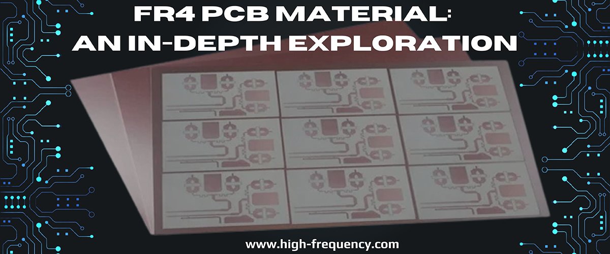
In terms of price, FR4 is the least expensive compared to dedicated high speed materials and Teflon, with Teflon being the most expensive. Though, FR-4 starts to drop off in performance when signal speed edges above 1.6ghz.
Newer generation substrates, Teflon, and flex circuits are the best options when it comes to Dk, Df, water absorption, and survivability in the environment
If a printed circuit board requires a frequency above 10GHz, newer generation substrates, Teflon, and Flex substrates are your best option since they are far superior to traditional FR-4 material.
The most common suppliers of high speed substrates are Rogers, Isola, Taconic, Dupont, and Megtron materials by Panasonic. All of these materials typically are lower Dk and lower loss.
Applications for HF PCBs
High frequency rigid and flex PCBs are used in many products and across many industries, including:
--- Cell phone
--- Telecommunications
--- Military and aerospace
--- RF microwave
--- Automotive (mainly LIDAR, which is a mini radar that communicates a vehicle’s surroundings)
--- High-density interconnect and high-speed design applications
 High-Frequency PCB: A Key Comp
 High-Frequency PCBs Design, Ma
 Miniaturization and High-Densi
 FR4 PCB Material An In-Depth E
