High-speed PCB design: PCB form factor design
PCB form factor design is critical, it will directly affect the later circuit board SMT mounting, board assembly and board division of the manufacturing process. Reasonable PCB board shape design can improve the late SMT placement of production efficiency and product yield.
1 external dimensions
All the PCB profile must be straight, which can reduce the PCB in the SMT process on the board, out of the board and midway transmission process error rate, thus shortening the PCB transmission time, enhance the PCB fixed and improve the quality of SMT processing.
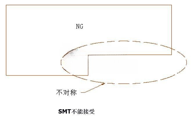
Enhance PCB fixation and improve SMT processing quality by adding a Dummy PCB in the free space as shown in the figure below.
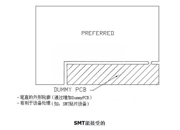
2 SMT equipment and production line can accept the maximum PCB form factor
SMT equipment can accept the maximum allowable form factor:
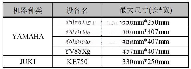
The maximum permissible external dimensions acceptable for SMT lines:

Considering the versatility of SMT production, it is recommended that the length*width of the Layout PCB board is not greater than 330mm*250mm, and the minimum size is not less than 50mm*50mm.
3 PCB positioning holes and restricted areas
Tooling holes on the PCB:
Tooling holes are two positioning holes on the PCB, which are used for mounter to fix the PCB better to facilitate the accurate mounter.
The basic specification of Tooling holes on single-sided PCB:
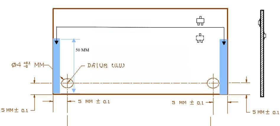
1) Tooling holes should be located on the longest side of the PCB to minimize angular differences;
(2) Tooling holes round hole diameter should be: 4mm +0.1/-0;
(3) Tooling holes elongated hole size: width of 4mm +0.1/-0, length of 5mm;
(4) For the PCB, each piece of small board data must be uniformly located in the lower left corner of the Tooling holes round holes as a benchmark;
(5) The distance between the two Tooling holes on the PCB should be the maximum separation allowed by the length of the PCB;
The basic specification of Tooling holes for double-sided PCBs:
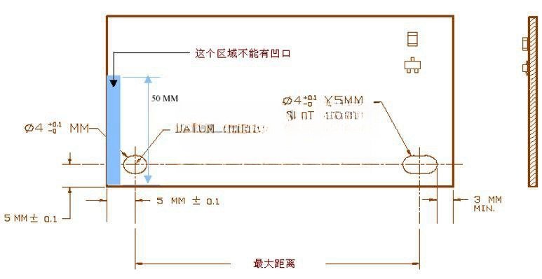
1) Tooling holes should be located on the longest side of the PCB to minimize angular differences;
(2) Tooling holes round hole diameter should be: 4mm +0.1/-0;
(3) For the PCB, the data of each small board must be uniformly located in the lower left corner of the Tooling holes as a reference, and symmetrical on both sides;
4) The distance between the two Tooling holes on the PCB should be the maximum separation allowed by the length of the PCB;
PCB board components mounted on the restricted area (single and double-sided PCB ):
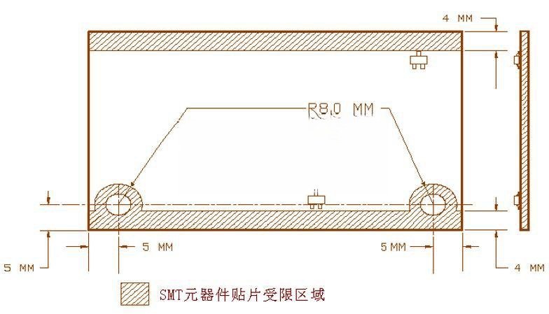
4 components, pads, lines in the Layout considered the definition of the restricted area
All components, pads and lines in the Layout PCB with the edge of the PCB have a minimum interval, in order to avoid damage in the sub-panel and handling process.
A. Minimum spacing between pads and lines and the edge:
1) Minimum spacing between the V-CUT: 0.5mm
2) Minimum spacing between pads and punched holes: 0.3mm
3) Spacing between and internal lines: 0.25mm
4) Minimum spacing from the edge of the stamp hole: 1.27mm
B. Minimum spacing between components and edges:
1) Minimum spacing from V-CUT: 1.27mm In case of through-hole components: 2.0mm
2) Minimum spacing from punched holes: 0.3mm
3) Spacing from internal wiring: 0.5mm
4) Size 1820 components and larger components and the minimum interval between the edge of the PCB should be: 10mm
5 PCB assembly and board separation
PCB circuit boards usually have a single-sided patchwork, family patchwork (family panel), double-sided patchwork (yin and yang patchwork) and other three types of patchwork.
5.1 General requirements for single-sided boards:
A. single-sided board should be arranged in the same direction, which is conducive to reducing the SMT program to do the steps and facilitate the use of machine fixation.
B. If there is a component in the board that exceeds the edge of the board, then the adjacent board must be considered to avoid the position, as shown below:
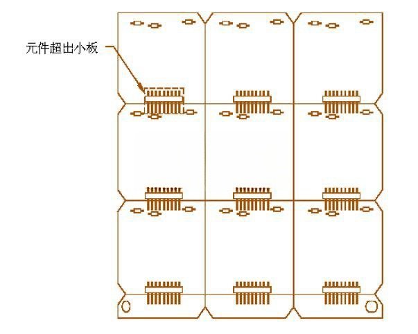
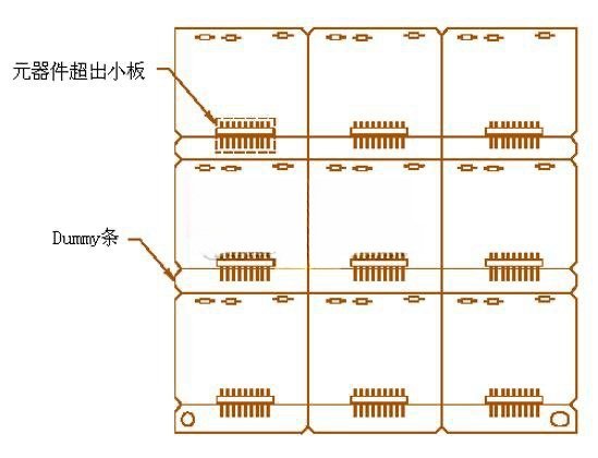
If there is no way to avoid the position of the small boards, it is also possible to avoid the position by adding a dummy strip between the small boards. Use additional dummy strips to increase the ease of PCB transfer and depaneling during the placement process. See the diagram below:
5.2 family panel (family panel ):
Family panel: that is, all the boards of a product are lined up in a PCB board, as shown.
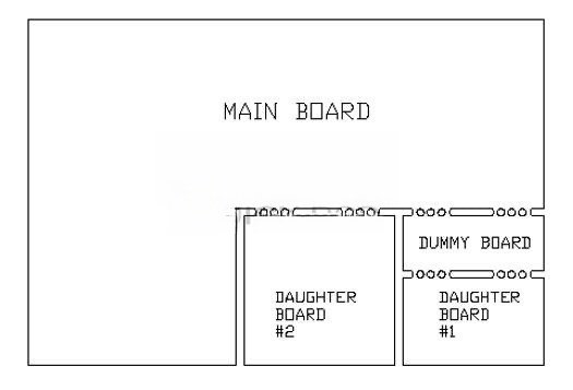
Advantages of the family style of board piecing:
1) Reduced number of boards, which facilitates purchasing;
2) Reduced WIP inventory;
3) Reduced Tooling costs for PCB manufacturing and SMT assembly;
4) Shorten the manufacturing cycle, also shorten the quality feedback cycle;
Disadvantages of family style PCB:
1) Compared with the standard PCB, the family-style PCB is poorer in terms of PCB raw material utilization, resulting in more Dummy board;
2) The family-style PCB is limited to boards with the same material and manufacturing process;
3) Increase the difficulty of processing and testing process;
4) The increase in the number of component types leads to insufficient feeding stations for SMT machines.
5.3 Double-sided boards (Yin-Yang boards):
Yin-yang board: Distribute the components of AB side on the same panel.
Advantages of yin-yang board:
1) Reduces the number of boards and facilitates purchasing;
2) Reduced WIP inventory;
3) Reduced Tooling costs for PCB manufacturing and SMT assembly;
4) Reduced manufacturing cycle time, also shorten the quality feedback cycle;
5) Unlike the family type PCB, it does not produce a redundant Dummy board;
Disadvantages of Dummy Board:
1) Increase the difficulty of reflow soldering;
2) The increase in the number of component types leads to insufficient feeding stations for SMT machines.
6 V-CUT + SLOT and Biscuits design
6.1 Biscuits design on FR-4 PCB material:
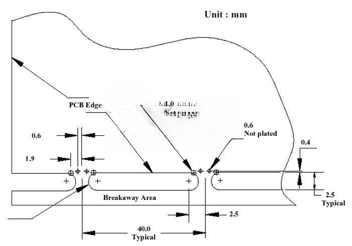
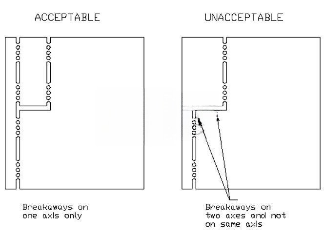
Biscuits designs need to be taken care of when dividing the board:
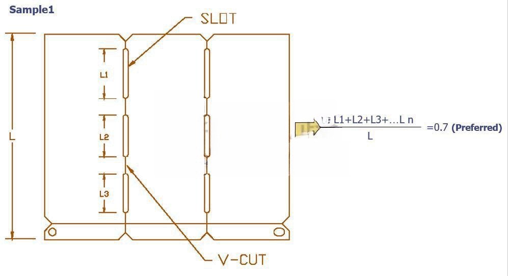
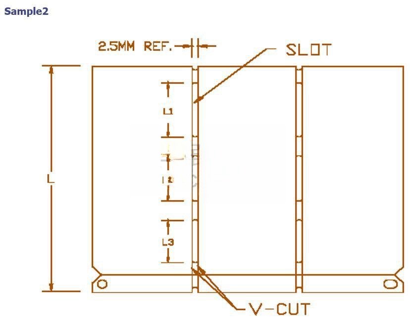
6.2 V-CUT+SLOT Design:
 High-Frequency PCB: A Key Comp
 High-Frequency PCBs Design, Ma
 Miniaturization and High-Densi
 FR4 PCB Material An In-Depth E
