RF PCB assembly: PCB Layout and Component Assembly Design Specifications
After assembling and patching the PCB board, above the electronic components are scattered, seemingly chaotic, but there is a big article.
The orientation of each electronic component, layout, PCB designers have to consider a lot of factors, to arrange them in a clear way after the PCBA factory in order to arrange production. Otherwise, a careless, will eventually cast a big mistake.
Below, follow the editor together with the “secret” to see how the engineers are to these electronic components, “home”.
PCB Layout and component assembly
1 General considerations (Layout and components)
Complex PCB board, covered with large and small chips and a variety of large and small components. How to ensure that each electronic component layout, heat dissipation is reasonable, the soldering of the solder joints firmly. In the process of production, transportation of each component is not subject to external forces and lead to false soldering, desoldering and so on.
In order to solve the above problems, in the design stage, we have to fully consider the PCB material, size, thickness and the type of electronic components mounted and other factors.
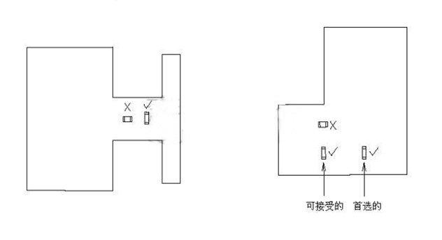
1.1 In the layout of the PCB should be considered in accordance with the component length and PCB vertical direction, especially to avoid components in the cloth is not solid, high stress parts to avoid components in the welding, board, vibration when the rupture. Specifically see the following diagram:

1.2 Component thermal expansion mismatch
Surface mount components, especially lead-free components in the welding process is the most important factor in the impact of thermal expansion, component welding end and component body if the high temperature welding and high current flow thermal expansion mismatch will lead to component body and welding end rupture. In general, large components are more susceptible to the impact of thermal expansion and contraction than small components, generally in the welding process only allows capacitance size equal to 1812.
2 Component Assembly
2.1 Component Patch
Similar components should be neatly arranged in the same direction on the PCB board to facilitate SMT placement, inspection, welding. It is recommended that all the direction of the components on the body of the direction of the label in the PCB board is the same arrangement.
2.2 SMT components hand soldering, filler soldering requirements:
As most of the SMT components in the hand soldering process is very susceptible to thermal shock and damage, so do not allow the SMD material for hand soldering, in the production of bad should try to solder at low temperatures.
2.3 SMT components should not be placed in the DIP (Double in-line package double direct assembly), through-hole components below (at present, the company does not have Beacon welding process to manual alternative, this article may not be implemented).
2.4 SMT material should be away from the PCB positioning edge 5mm
2.5 SMT processing must be matched with the welding process, such as reflow soldering is only applicable to PCBA reflow soldering, wave beacon welding is also only applicable to PCBA wave beacon welding.
3 wave beacon welding (temporarily omitted)
interested partners can continue to pay attention to the editor, I will be in the right time to fill you in.
4 Reflow soldering
4.1 Reflow conditions:
In order to ensure the consistency of the performance of components before and after reflow soldering, it is required that the parameter requirements of the components must meet the reflow requirements of HYT.
Reflow soldering temperature profile:
Ramp rate (Ramp rate): > 4C ° / Sec
Peak temp.: 235 C° (lead product) 270 C° (lead-free product)
Liquefaction time (Time above liquidus): should be able to withstand 120Sec.
4.2 Component spacing:
PP- Pad to Pad
BB- Body to Body
BP- Body to Pad
4.3 Line Layout
4.3.1 Use insulating and non-solderable materials to cover the exposed, non-solderable copper cladding and wiring to prevent solder from flowing onto the exposed copper cladding and wiring during reflow soldering and resulting in a tinless pad, less tin or soldering errors.
4.3.2 Pad Symmetry
Avoid connecting pads with large copper foils or minimize the connection between pads and large copper foils with heat insulating materials to avoid cold soldering due to rapid heat dissipation during reflow soldering.
For single shaped components, the pads should be designed symmetrically to avoid the phenomenon of monument during reflow soldering.
4.3.3 Design Guidelines for Through-Hole Positioning
The through-hole should be far away from the pad of the component so that the solder will not flow out of the pad through the through-hole during reflow soldering, resulting in tinlessness, less tin, and so on. The minimum distance between the through-hole and the pad is 0.63mm.
Through-holes are only allowed on the pads of large components, such as DPAK & D²PAK, but the diameter of the through-hole must not be larger than 0.3mm or smaller, and in order to avoid tin flowing through the through-hole to the other side of the pads during reflow soldering and causing bumps on the other side of the pads, it should be considered that the through-hole should be plugged on the other side of the pads.
4.4 Reflow Assembly Requirements
4.4.1 Soldering with mechanical support devices:
Provide more solderable area of copper foil on the PCB to provide sufficient mechanical strength to support the soldering points between the component and the PCB, especially where the wire meets the copper foil.
4.4.2 Assembly of Special Components.
a. In the soldering process (especially the lead-free process), do not use components that do not match the thermal expansion of the PCB and have a large thermal expansion, as board distortion and cracking of the solder joints may occur and affect reliability unless a successful test has been verified and no problems have been identified.
b. In the reflow soldering process, unless it has been confirmed that the test is successful and confirmed that the results are not harmful, or do not choose non-SMT materials in the SMT surface assembly in the furnace after manual tin.
c. Of course, some components can be soldered as SMT materials by correcting their pins.
d. When non-SMT components used in SMT SMD, the pin curvature and flatness have certain requirements, if you need to bend, the bending part can not be extended to the feet and the body of the joint, but the bending point and the distance from the body (L) for the diameter or thickness of the component pins, but at least can not be less than 1.0mm, refer to the following charts and tables:
If its pins are leveled, the thickness of the leveling shall be not less than 40% of the pin diameter:
e. Co-planarity requirements for shaped component pins (maximum 0.15mm)
 High-Frequency PCB: A Key Comp
 High-Frequency PCBs Design, Ma
 Miniaturization and High-Densi
 FR4 PCB Material An In-Depth E
