High-speed PCB design: PCBA design specifications you should know
In this paper, we will focus on the limitations of the component form, automatic insertion of components cut rivet shape, the density of the component layout, pads, machine insertion of the component labeling and other design requirements in order to develop.
First, the limitations of the component form
1. Horizontal insertion of components: as shown in Figure 9, the component shape for the following restrictions
Length L = 3.0mm ~ 10mm
Body diameter D = 0.6mm ~ 4.0mm
Lead diameter d = 0.4mm to 0.8mm
Jumper L = 5.5mm to 30mm
2. Vertical insertion element: As shown in Figure 10, the element body can be accommodated up to a maximum height of 23mm and a maximum diameter of 13mm.

Second, the automatic insertion of the shape of the rivet cutting components
1. Horizontal insert element: its shape in the printed board cut rivets shown in Figure 11a, where CL = 1.5-2.0 ± 0.5mm, CA = 0-35 ± 10 ° adjustable, h ≈ 0.1mm.
2. Vertical insertion element: the shape of the cut rivets on the printed board is shown in Figure 11b, where CL=1.5-2.0±0.3mm, CA=0-35±10°adjustable.
Third, the maximum allowable density of component layout
1. lying inserted components: a variety of the densest possible layout of its adjacent minimum spacing shown in Figure 12....
2. Element density requirements:
The greater the component density on the PWB, the smaller the self-insertion machine alignment, and therefore the higher the efficiency. However, component density is too large when inserting will bruise and interrupt neighboring components and damage the tool. The following chart shows the maximum density that the insertion machine can accept:
3. Density Requirements for Horizontal Components and Patches
3.1. Component body, component lead angle and SMT patch component minimum distance for the circumference of 3mm
3.2. Parts foot bending degree: 15-45 degrees (adjustable)
4. Component copper skin design.
Self-insertion machine insertion, should prevent the following problems.
(1). Component angle is too large, easy to drop and produce floating feet
(2). Component angle is too small, easy and neighboring copper short-circuit The method is as follows
5 Horizontal component hole skew range.
Vertical inserted components:
(a) vertical insert components should be arranged to consider the components have been lying inserted into the impact of vertical insert components, should also be avoided when the vertical insert components pins outward molding may be caused by neighboring components pin soldering (directly touching or over the wave soldering when hanging tin), as shown in Figure 13.
(b) vertical insert components of the densest row of adjacent vertical insert components of the body (including pins) the minimum distance between the body should not be less than 1mm, vertical insert components and lying insert components should be appropriate spacing between. As shown in Figure 14.
(c) Density between vertical components and SMT components:
Four, Front and back Density between SMT components and vertical components
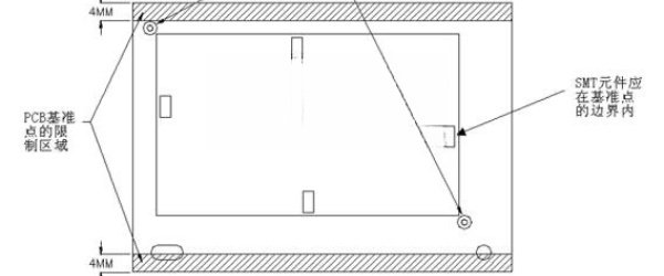
As the vertical insertion machine components cut off the foot bending parts in the vertical insertion will be with the PCB front and back have a closer distance, for this reason on the front and back of the SMT components and vertical component hole distance has requirements.
1. (W)4mm×(L)9mm Range cannot have SMT components。
2. (W) 10mm × (L) 16mm, there can be no SMT components with a height of more than 1mm.
3. (W)13mm×(L)22mm: No SMT components with a height greater than 5mm.
4. The height of the components on the upper and lower planes must not be greater than 6mm.
Five, the pad
1. The design of the pad should take into account the direction of the component pins cut riveting forming, should be conducive to welding, should take into account the wave soldering when the component pins are not shorted with the adjacent printed circuit.
2. Horizontal plug components of the pad should be designed into a long round, jack position in the pad as shown in Figure 15a; vertical plug components of the pad should be designed into the jack and pad for the round, jack position as shown in Figure 15b.
Six, organic plug components
all organic plug components should be labeled in the marking symbols on the chart on the bit number, including short-circuit jumpers, rivets, need to be machine-inserted pins, etc., rivets, pins need to be each hole in each pin labeled bit number, short-circuit jumper, rivets, pins can be labeled only in the face of the component.
 High-Frequency PCB: A Key Comp
 High-Frequency PCBs Design, Ma
 Miniaturization and High-Densi
 FR4 PCB Material An In-Depth E
