RF PCB Stack-Up: Best Practices for Signal Integrity and Performance
The stack-up of an RF (radio frequency) PCB (printed circuit board) is critical for ensuring optimal performance in high-frequency applications. A well-designed stack-up can significantly affect signal integrity, impedance control, and overall functionality of RF circuits.
Main Structure for RF PCB Stack-Up
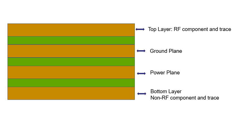
An RF PCB stack-up typically consists of multiple layers, each serving a specific function:
Signal Layers: These layers carry RF signals and are typically located in the center of the stack-up. They may include microstrip or stripline configurations, depending on design requirements.
Ground Plane: A solid ground plane is essential for shielding and maintaining a consistent reference point for signal layers. It helps minimize electromagnetic interference (EMI) and supports effective impedance control.
Power Distribution Layers: These layers provide power to RF components and help distribute it evenly, which is vital for performance and reliability.
Dielectric Material: The materials used between layers (dielectric substrates) significantly impact the electrical characteristics of the PCB. Common materials include FR-4, Rogers, and PTFE, chosen for their low loss and stable dielectric constants.

Important Factors to Consider When Designing RF PCB Stack-Up
When designing an RF PCB stack-up, several key factors must be considered:
1. Impedance Control: Ensuring that the impedance of the signal traces matches the required values (usually 50 or 75 ohms) is crucial for minimizing signal reflections.
2. Dielectric Thickness: The thickness of the dielectric material between layers affects the overall performance, including capacitance and signal velocity. Designers must calculate the optimal thickness to achieve desired electrical properties.
3. Layer Arrangement: The order of signal, ground, and power layers must be thoughtfully planned to maintain signal integrity and reduce EMI. Ground planes should be placed close to signal layers for optimal shielding.
4. Thermal Management: Considering how heat will dissipate through the stack-up is essential for high-power RF applications. Adequate thermal vias and copper pours can enhance heat dissipation.
5. Manufacturability: The complexity of the stack-up can impact manufacturing processes. Designers must ensure that their stack-up can be fabricated within the capabilities of the chosen PCB manufacturer.
Challenges of Manufacturing a Multilayer RF PCB Stack-Up
Manufacturing multilayer RF PCBs poses several challenges:
1. Precision Alignment: Ensuring precise alignment of layers during fabrication is crucial for maintaining signal integrity. Misalignment can lead to impedance mismatches and degraded performance.
2. Layer Count: Increased layer count can complicate manufacturing processes and raise costs. Each additional layer requires careful planning to ensure effective routing and performance.
3. Material Variability: Variations in dielectric materials can affect performance. Consistency in material properties is essential for predictable RF behavior.
4. Complex Drilling and Via Design: The use of blind and buried vias can complicate manufacturing. Designers must balance via usage with the need for high-frequency performance, as poorly placed vias can disrupt signal integrity.
5. Testing and Validation: Implementing thorough testing procedures for multilayer stack-ups is essential but can be resource-intensive. Ensuring that all layers meet specifications before final assembly is vital for product reliability.
Conclusion
The stack-up of RF PCBs is a foundational aspect of their design and performance. By understanding the main structure, key design considerations, and manufacturing challenges, engineers can create effective RF PCB stack-ups that optimize signal integrity and reliability across a variety of applications. Proper planning and execution are essential for achieving the best performance in high-frequency electronics.
 High-Frequency PCB: A Key Comp
 High-Frequency PCBs Design, Ma
 Miniaturization and High-Densi
 FR4 PCB Material An In-Depth E
