
The Heartbeat of Modern Electronics: Unveiling the Power and Innovation Behind PCBs

Discover how Printed Circuit Boards (PCBs) power the devices you love. Explore their design, types, applications, and future trends in this in-depth guide. Perfect for tech enthusiasts and industry professionals!
Introduction: The Unsung Hero of Every Gadget:
From smartphones to satellites, Printed Circuit Boards (PCBs) are the silent workhorses that make modern electronics possible. These intricate boards connect components, transmit signals, and ensure your devices function flawlessly. But what exactly are PCBs, and why are they so revolutionary? Let’s dive into the world of PCBs and uncover their secrets.
What is a PCB? The Backbone of Electronics:
A Printed Circuit Board (PCB) is a flat, laminated structure made of non-conductive materials (like fiberglass) with conductive copper pathways etched onto its surface. These pathways, or traces, act as highways for electrical signals, connecting components like resistors, capacitors, and microchips. Think of a PCB as a city’s infrastructure: roads (traces), buildings (components), and power lines (copper layers) working together seamlessly.
A Brief History: From Wire Chaos to Silicon Precision:
Before PCBs, electronics relied on tangled webs of wires, making devices bulky and prone to failure. The invention of PCBs in the 1940s revolutionized electronics by enabling compact, reliable designs. Today, advancements in materials and manufacturing have pushed PCBs into everything from wearables to AI-powered systems.
Types of PCBs: Choosing the Right Board for the Job:
Not all PCBs are created equal. Here’s a breakdown of common types:
1. Rigid PCBs: Found in most devices (e.g., laptops, TVs), made of sturdy FR-4 fiberglass.
2. Flexible PCBs: Bendable boards for wearables and medical devices.
3. Rigid-Flex PCBs: Hybrid designs for aerospace and military applications.
4. High-Frequency PCBs: Optimized for 5G, radar, and RF systems.
5. HDI PCBs: Ultra-compact boards with microvias for smartphones and IoT devices.
How PCBs Are Made: From Concept to Reality:
The PCB manufacturing process is a blend of art and science:
1. Design: Engineers use software like Altium or KiCad to create schematics and layouts.
2. Imaging & Etching: UV light transfers designs onto copper-clad boards; chemicals etch away excess copper.
3. Drilling & Plating: Precision drills create holes for components, later plated with conductive material.
4. Layering: Multi-layer boards are pressed together under high heat.
5. Testing: Automated Optical Inspection (AOI) and electrical tests ensure quality.
Applications: Where Would We Be Without PCBs?
PCBs are everywhere:
- Consumer Tech: Smartphones, gaming consoles, and smart home devices.
- Healthcare: MRI machines, pacemakers, and glucose monitors.
- Automotive: Self-driving car systems, EV battery management.
- Aerospace: Satellite communication and navigation systems.
The Future of PCBs: Innovation on the Horizon:
1. 3D-Printed PCBs: Rapid prototyping with additive manufacturing.
2. Embedded Components: Chips and resistors integrated directly into the board.
3. Eco-Friendly PCBs: Biodegradable substrates and lead-free soldering.
4. AI-Driven Design: Machine learning optimizes layouts for speed and efficiency.
Why PCBs Matter: Sustainability and Security Challenges:
- E-Waste: Over 50 million tons of e-waste are generated yearly. Recycling PCBs is critical but complex due to toxic materials.
- Security: Counterfeit components and tampering risks drive demand for secure, traceable PCBs.
PCBs are more than just green boards—they’re the foundation of our digital world. As technology evolves, so will PCBs, enabling smarter, faster, and greener electronics. Whether you’re a hobbyist or a tech giant, understanding PCBs is key to unlocking tomorrow’s innovations.
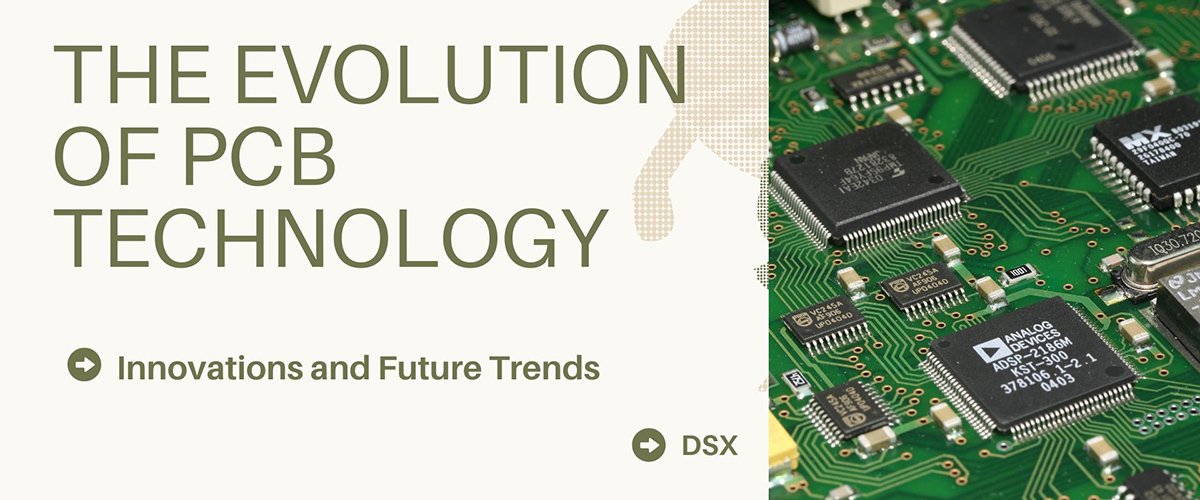 The Evolution of PCB Technolog
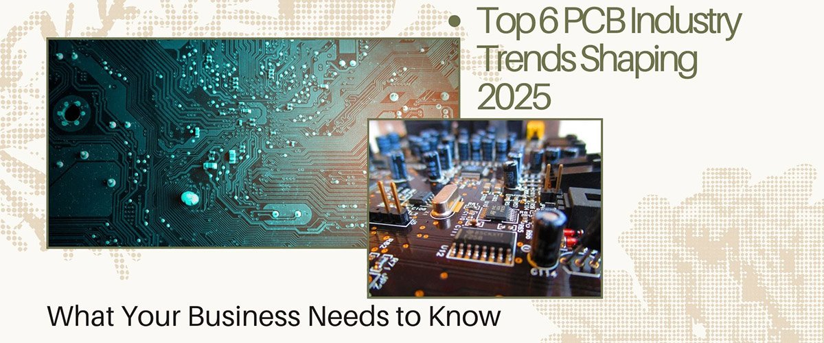 Top 6 PCB Industry Trends Shap
 Sustainable Materials and Manu
 The Impact of DeepSeek, NVIDIA